Skip to content
Electronics · Physics

P–N Junction Diode Simulation

Electrons and holes at a p–n junction: watch the depletion layer form, shrink in forward bias and widen in reverse. Plot the I–V characteristic of silicon, germanium, a Zener and an LED.

Interactive virtual lab · no download · works on phones and laptops

Chapter
Semiconductor Electronics
For
Class 12 · JEE · NEET
Time
~12 min

P–N Junction Diode is a Pro simulation

Pro opens all 125 virtual labs — 483 simulations with guides and quizzes.

How to use it

  1. 1Choose forward, unbiased or reverse, and set the battery voltage.
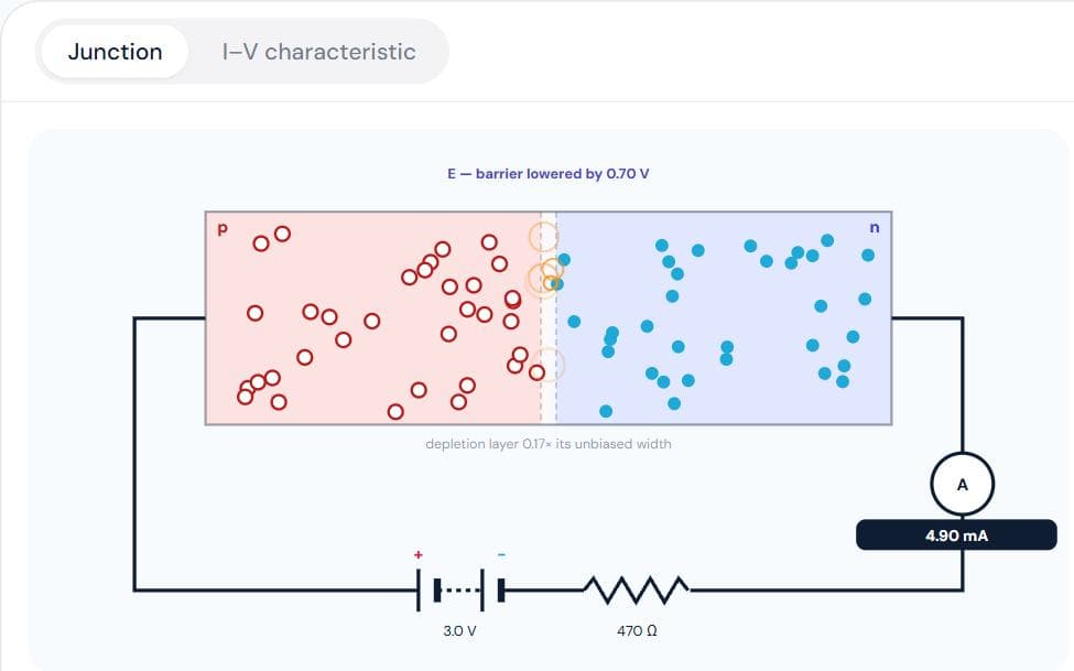
  2. 2Watch the carriers, the depletion layer and the ammeter.
  3. 3I–V tab: sweep the voltage and see the operating point move on the curve.
  4. 4Change the diode type to compare Si, Ge, Zener and LED.

What to notice

  • Carriers diffuse across the junction and recombine, leaving fixed ions: the depletion layer and its barrier potential (~0.7 V for Si, ~0.3 V for Ge).
  • Forward bias pushes carriers into the junction: the layer narrows and current rises steeply past the knee voltage.
  • Reverse bias pulls carriers away: the layer widens and only a tiny leakage current flows — until breakdown.
  • A Zener diode is built to break down at a set reverse voltage and hold it there.

For teachers

A ready-made teaching kit comes with this lab

  • Lesson plan

    21 min, 4 steps

  • Ask the class

    4 questions with answers

  • Quick quiz

    7 questions, printable

  • Key formulas

    2 formulas

About the P–N Junction Diode simulation

Join p-type and n-type silicon and electrons and holes diffuse across the junction and recombine, leaving a thin depletion layer of fixed ions with no free carriers. The ions' field creates a barrier potential — about 0.7 V for silicon and 0.3 V for germanium. Forward bias lowers the barrier and current rises steeply; reverse bias widens the layer and only a tiny leakage current flows, until breakdown.

In this p–n junction diode simulation you set the battery to forward, unbiased or reverse, change its voltage and the series resistor, and watch the depletion layer, the carriers and the ammeter. The I–V characteristic screen plots the curve with a load line and operating point for silicon, germanium, a Zener and an LED. It covers Semiconductor Electronics in Class 12, JEE and NEET.

Also covers: diode, p-n junction, forward bias, reverse bias, depletion layer, barrier potential, I-V characteristic, Zener diode, LED, knee voltage, rectifier.
Frequently asked questions

What is forward bias?

Connecting the p-side to the battery's positive terminal and the n-side to the negative, which lowers the barrier and lets current flow.

What happens to the depletion layer in reverse bias?

It widens, and only a very small reverse current flows.

What is the knee voltage of a silicon diode?

About 0.7 V — the forward voltage at which the current starts rising steeply.

What is a Zener diode used for?

Voltage regulation: in reverse breakdown it holds an almost constant voltage over a wide range of current.