Skip to content
Electronics · Physics

n-type & p-type Semiconductor (Doping) Simulation

Build a silicon crystal atom by atom. Drop in phosphorus or arsenic and a spare electron is set free; drop in boron or gallium and a hole appears. Heat it, apply a voltage, and make a p–n junction.

Interactive virtual lab · no download · works on phones and laptops

Chapter
Semiconductor Electronics
For
Class 12 · JEE · NEET
Time
~10 min

Doping: n-type & p-type Semiconductors is a Pro simulation

Pro opens all 125 virtual labs — 483 simulations with guides and quizzes.

How to use it

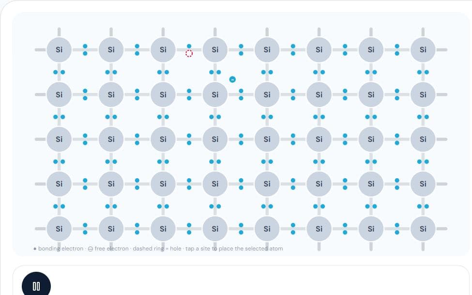
  1. 1Pick an atom in the palette, then tap a site in the crystal to replace the silicon there.
  2. 2Turn up the temperature to break bonds and make electron–hole pairs.
  3. 3Switch on the battery to see electrons and holes drift in opposite directions.
  4. 4Use “Make a p–n junction” to dope the left half p-type and the right half n-type.

What to notice

  • Each silicon atom shares its 4 valence electrons in 4 covalent bonds.
  • A pentavalent donor (P, As) has one electron too many: n-type, electrons are the majority carriers.
  • A trivalent acceptor (B, Ga) leaves a bond one electron short — a hole: p-type, holes are the majority carriers.
  • The crystal stays electrically neutral: doping adds carriers, not net charge.

For teachers

A ready-made teaching kit comes with this lab

  • Lesson plan

    19 min, 4 steps

  • Ask the class

    3 questions with answers

  • Quick quiz

    6 questions, printable

  • Key formulas

    2 formulas

About the Doping: n-type & p-type Semiconductors simulation

Pure silicon is a poor conductor: each atom shares its four valence electrons in bonds with four neighbours, leaving few free carriers. Doping replaces a tiny fraction of the atoms. A pentavalent atom such as phosphorus or arsenic brings a fifth electron that is free to move (n-type); a trivalent atom such as boron or gallium leaves a bond one electron short — a hole that behaves like a positive carrier (p-type).

In this doping simulation you tap boron, gallium, phosphorus or arsenic into a silicon crystal, watch free electrons and holes appear, raise the temperature to break bonds into electron–hole pairs, connect a battery to make them drift, and dope one half p-type and the other n-type to start a p–n junction. It covers Semiconductor Electronics in Class 12, JEE and NEET.

Also covers: doping, n-type, p-type, semiconductor, silicon, holes, free electrons, donor, acceptor, pentavalent, trivalent, intrinsic, extrinsic, diode making.
Frequently asked questions

What are the majority carriers in n-type silicon?

Free electrons, donated by pentavalent atoms such as phosphorus or arsenic.

Is a p-type semiconductor positively charged?

No. It is electrically neutral overall: every hole comes from a neutral acceptor atom.

Why does a semiconductor conduct better when hot?

Heat breaks more bonds, freeing more electrons and holes.